2.0mm 14 Layer HDI PCB Board Prototype FR4 TG170 Green Solder Mask
HDI PCB Board 14 Layer PCB Board Green PCB Board Prototype Circuit Board Prototype Circuit Board FR4 PCB Board
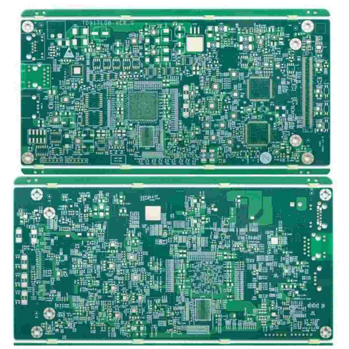
14L 1+N+1 HDI Boards
High density interconnect printed circuit boards, which are also called HDI boards, are characterized by finer lines, closer spaces, and more dense wiring.
HDI boards own higher circuit density, its designs can include not only smaller through holes and capture pads, but also higher connection pad density. They are widely used to reduce the weight and overall dimensions of products, as well as to enhance the electrical performance of the device.
HSX products cover 1~32L FR-4 PCB, IMS PCB,HDI Boards, high frequency PTFE boards and Rigid-flex boards etc. It provides flexible quick turn production services (12 hours to72 hours), as well as small volume to big volume PCB manufacturing.
The panel size of HSX factory's capability is max 740x500mm, but when the panel size is larger than 600mm, it will need to be review at first. And the minimum panel size that we can reach is 5*5mm.
The PCB thickness we can reach is from 0.2mm to 4.0mm, if the board thickness is smaller than 0.2mm, or bigger than 4mm, will need to evaluate the board at first(PS. if board thickness </= 0.6mm, the surface finished can not be HASL/LF-HASL)
Factory's minumun hole size capability is 0.15mm, if the hole size is smaller than 0.15mm, will need to review the board at first.
The solder mask colors include, red, matt green,matt green,blue,matt blue,black,matt black,white, and so on.
The colors of leged include white, black and so on.
| Circuit board Layer count: | 14L | Circuit board laminate: | FR4 TG170 |
| Layer Copper thick: | Outer 1oz Inner H oz | Board thickness: | 2.0MM |
| Smallest hole size: | 0.20mm | Smallest PCB track/gap: | 4/6mil |
| Solder mask color: | TAIYO Green | Silk screen color: | White |
| PCB surface finished: | Immersion Gold | Board profile: | Routing |
| PCB Board Application: | digital products |
| Requesting Special requirement: | HDI Buried vias and blind vias, one step stack up /impedance control/resin filled and plated over/0.25mm BGA |

FAQ:
Q1:Are you a factory or trade company?
A: Yes, we are the factory, we have independent quick turn prototype PCB manufacturing & big volume PCB production lines.
Q2:What kind of PCB file format can you accept for production?
A: Gerber, PROTEL 99SE, PROTEL DXP, POWER PCB, CAM350, ODB+(.TGZ)
Q3:If we have no PCB file/Gerber file, only have the PCB sample,can you produce it for me?
A: Yes,we could help you to clone the PCB. Just send the sample PCB to us, we could clone the PCB design and work out it.
Q4:What is your standard lead time for PCB?
A: Sample/prototype(less than 3sqm):
1-2 Layers: 3 to 5working days (fastest 24hours for quick turn services)
4-8 Layers: 7~12 working days (fastest 48hours for quick turn services)
Mass production (less than 200sqm):
1-2 Layers:7 to 12 working days
4-8 Layers:10 to 15 working days
Q5:What is your min. order quantity?
A: There is no MOQ.The quantity will only affect the price.
Q6. How to get quick quotation?
Please provide gerber file and details of the board(including layer, board thickness, copper thickness, surface treatment, solder mask and silkscreen color, special request if any, demand quantity, etc)
sample:
| PCB Type | 4L multilayer PCB |
| Surface finished | LF-HASL |
| Base material | FR4, TG170 |
| Copper thickness | 1oz inner base, 1oz finished copper |
| PCB solder mask | Green for both sides |
| PCB silkscreen | White for both sides |
| Special requirement | Resin plugged hole/plating edge, gold finger thickness 30u" |
Product Tags:

|
|
2.0mm 14 Layer HDI PCB Board Prototype FR4 TG170 Green Solder Mask Images
|